

Major actual limits of the manufacturing facility
This paper aims the orientation of some product architecture aspects in order to improve the tune among delivery time, quality and charging of the implementation process and goods manufacture on WEGO systems.
Major actual limits of the manufacturing facility:
SMD Assembling:
- Usable area at the screen printer = 440mm x 440mm (Stencil of 23”)
- Sometimes it is not recommended the use of big panels, in order of the error enlargement possibility throughout the many panel’s boards. When possible, contact the technical team of WEGO Systems about the best option of panel assembling for your PCB.
- Panel width on Pick & Place of 102mm until 380mm.
- Panel length on Pick & Place of 80mm until 450mm.
- Thickness board of 0.4 until 4.5mm.
- Borders clear area (no components) of at least 5mm.
- Smallest passive component = 0402.
- Semiconductors = All of encapsulations.
- Double remelt on the Top & Bottom assembling.
- Unrestricted number of layers (until 10 layers) on PCB. For more than 10 layers contact the WEGO Systems technical group.
- Different quantities of items/pns = BOM evaluation required. Until 200 feeders of 8mm width and 10 different types of tray components.
- For Lead Free assembling contact WEGO Systems technical team.
PTH Assembling:
- All handmade encapsulations.
- By waves requires prior assessment.
- For Lead Free assembling contact WEGO Systems technical team.
Special Assembling:
- Contact WEGO Systems technical team.
PCB General Characteristics:
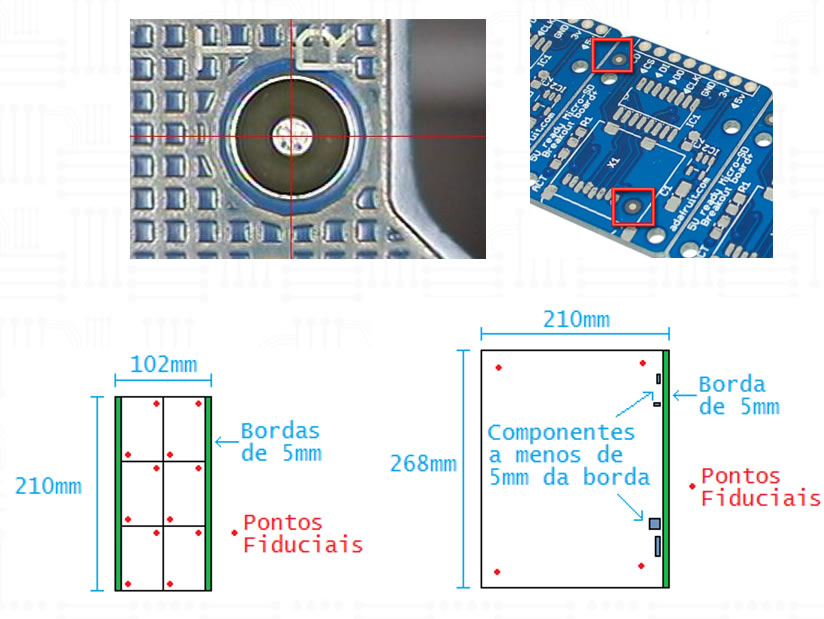
Fiducial Marks are used as reference for machines during the product handling. It is required the existence of at least two diagonally lined fiducial marks for each panel’s board.
.
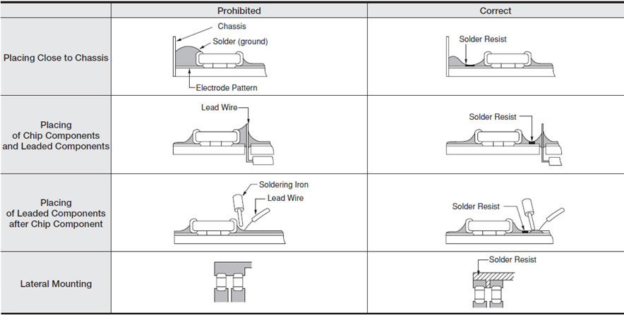
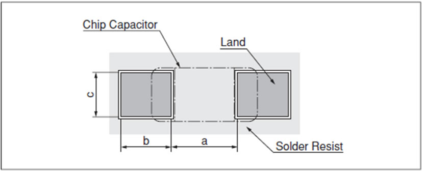
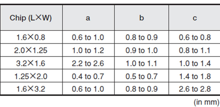
Pads/lands and epoxy masks (solder resists):
To look out if the pads and epoxy masks design follow the specified determinations of the datasheet of each component, in other words, according to the manufacturer specifications. The adequate compromise among the land size on the board, the component pad and the epoxy mask are going to determine if the solder will assemble the component to the board. Following there are some examples of how this factors are treated by the manufacturers:
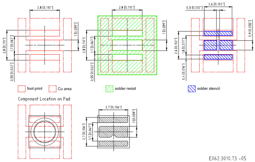
Example of muRata capacitors from Chip Ceramic line.
Example of OSRAM LEDs from OSLON Square line.
Localization and polarity markers:
The existence of a serigraphy mask indicating the localization of all the components on the board is highly recommended, as well as its polarities or desired positioning. When that’s not possible, there has to be an annex document which can clarify the doubts that will appear during assembling. Just the coordinates are not enough to clear all the possible questions that might occur.
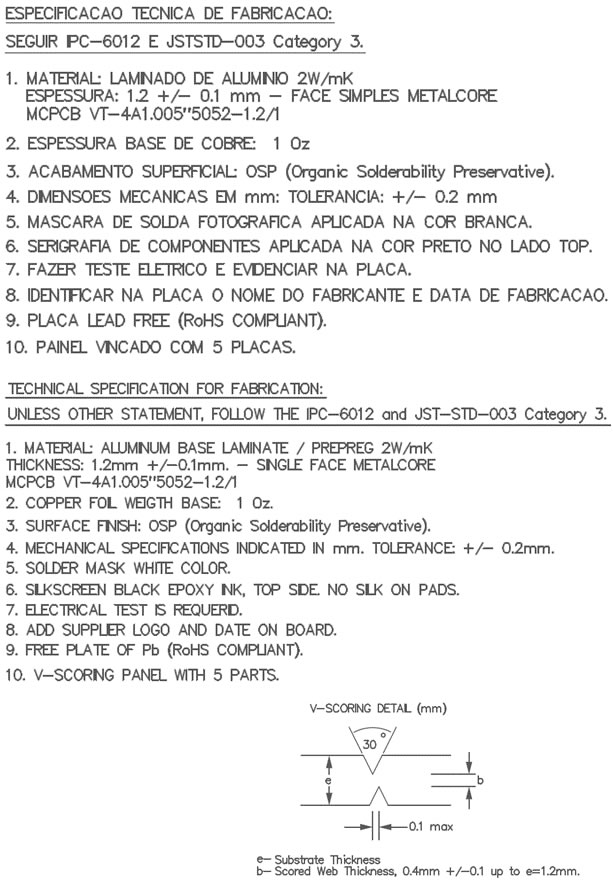
Board building specifications
Following the board documentation there must be all the required specifications for the manufacturer to build the PCB in a way that makes it possible to create it according to the project requirements. An example of specifications follows.
Other attentions:
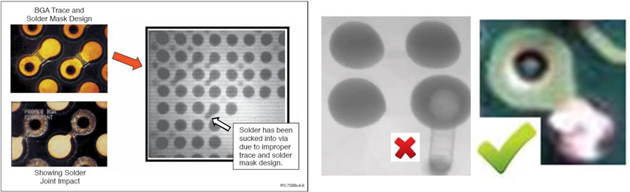
- Avoiding passing through holes directly on the components’ pads, under penalty of solder to be sucked into via. There must be an epoxy mask limiting the excursion of the solder by the land area.
DOWNLOAD HERE the Technical Disclosure speaking of “Main current limits of industrial structure”